This page is at least 5 years old !
Distropia (@Oshelete) sent me this peculiar board after I've asked publicly if anyone had bootleg NeoGeo MVS boards for sale, dead or alive.
Thanks to him !
It's worth noting that neo-geo.com forum member Nightmare Tony (RIP), who was an SNK US technician wrote that he had to dissect such a board at the time and found out that the custom chips were Texas Instruments ASICs. The particular board version he got hold of is unknown.
Such boards are rare to come across today but they have been known to exist for a while. Pictures of different versions (of possibly different manufacturers) can be found online, but I hadn't seen any of this one before.
It has the form factor of an MV1FZ and apparently full compatibility with the only two games I own: Metal Slug X and King of Fighters 99. Distropia also recalled that it ran his games without any problems. Amusingly, this board even has a few advantages over the legit version: there's a red LED to indicate when power is applied, the RTC and backup RAM battery causing corrosion damage on many original boards is replaced by a more chemically stable supercap, all ROMs are socketed, and the volume potentiometer is much more sturdy.
Here's the main board and the vertical slot board, which I desoldered for easier stripping:


There are no components on the back sides.
The soldermask color difference between the two boards is striking. Having both boards made by two different factories or assembly lines didn't make sense at first. By looking at the traces on the main board, I noticed that it had 4 layers, unlike the slot board which only had 2 !
Surprising for a bootleg (understand "cost optimized") system from the mid-90's. Maybe the reduced board size was one of their sales arguments.
Being familiar with the MVS architecture makes it easy to split the board in sections:

They didn't put any special effort where it wasn't needed: unlike SNK, they succeeded in making the board small enough without having to pack up the standard logic chips into ASICs. The 4-layer board obviously plays an important role here.
Some late games attempt to detect bootleg systems by running checks on startup, locking up if they find that the RTC or if the often unused higher part of VRAM were left out. They didn't go full cheapo with this board, everything is present so the checks would have probably passed (I didn't have those games to try it).
Probably because of the higher cost of assembling SMD components, they decided to use through-hole resistor arrays for the video DAC instead of the individual SMD resistors found on the MV1FZ. They're located right next to the pull-up arrays for the inputs above the JAMMA edge, which makes perfect sense.
Going into more details meant I had to beep some traces. Getting rid of the components was going to make following them by translucency easier, so the board got a nice hot air strip:

I didn't bother removing the DIP (!!) 68000 and the YM2610 because there weren't many traces vanishing underneath.
Prior to the strip, I had the components references written down on a simplified schematic to remember which went in each position. Shortly after, I noticed they were already conveniently printed on the silkscreen. Thanks...
Nothing very interesting was revealed apart from what appears to be a PCB manufacturing code under one of the custom chips: M064-007.

Here are some Motorola, UTC, TI, National, Hitachi, Lattice, Fujitsu, ST, Yamaha, AMD, Intel, UMC, Mitsubishi and NEC logic chips and memories ! The mix of so many different brands makes me believe they just went for the cheapest available, like leftovers from the nearest components dealer.
The four EPROMs were dumped and compared positively against the common ROM set found on MV1FZs:
- C16-01- is sp-s2.sp1 (CRC32 9036d879), the system ROM
- C16-02- is 000-lo.lo (CRC32 e09e253c), the sprite shrink lookup ROM
- C16-03- is sfix.sfix (CRC32 c2ea0cfd), the fix layer graphics ROM
- C16-04- is a cleaned up version of sm1.sm1, with every bytes above 0xF800 set to 0xFF
The six PAL20V8 were dumped but only gave bits set to 1 outside of their configuration field, meaning that they were read-back protected.
The bigger Lattice PLD was not dumped because I didn't have an adapter for it. It's probably also protected anyway.
The NEO-ZMC2 chip, used as a custom graphics serializer on original boards, was replicated with four of those PALs and four 74LS153 (dual 4-to-1 multiplexers). Each PAL is used as a shift register for one bitplane (8 bits), while the 74LS153s pick out which outputs are used for rendering according to the odd/even pixels flip and horizontal mirroring signals (4 possibilities).
I found that pretty clever, and it meant that the bootleggers didn't just copy the NEO-ZMC2 masks to make a new ASIC: they had to know exactly how the logic worked.
Speaking of ASICs, here are the only two custom chips used on the board:

Lucky coincidence, I'm Aries too ! This meant... nothing at all since astrology is bullshit.
Some of you might remember a brand of ZIF connectors named "Aries Electronics", but them having anything to do with MVS bootlegs is doubtful.
I'm quite confident that anyone with $50.000 can set up a company with a random name and have ASICs made if they wanted to.
The AR-1602B (QFP176) is interestingly referred to as "LSPC" on the board: Line SPrite Controller, the name that SNK used for the original chip. The second generation NeoGeo video chipset is normally constituted of two chips:
- LSPC2-A2, which contains almost all the video logic.
- NEO-B1, which is a simpler line-buffer chip, mostly containing RAM cells.
The AR-2081A (QFP208) is obviously playing the role of NEO-B1, but is called "CHIP23". Maybe "NEO" was too close to the "NeoGeo" trademark and they didn't dare using the name. Or maybe because this chip also contains logic for other parts of the system.
The markings are of the common COMPANY(AR)-REFERENCE(1602)-REVISION LETTER(A) kind but may just be bogus, as I also doubt they had a 1602A chip made before their 1602B. The reference number doesn't have to mean anything either if the company only ever had two custom chips made. Only the datecodes (which might have been added by the packaging company) could be legit. If that's the case, these chips were made in April of 1996.
Obviously, they weren't made by the bootleggers since producing integrated circuits is a very high-tech process. Like the original SNK chips, these had to be contract produced by some large semiconductor company which was probably never aware that this particular design was going to be used in a counterfeit system.
About identifying who made them, the packages only give a few clues. The features (marking type, font, ejector marks...) don't match Fujitsu, NEC or Toshiba parts. Looking for similar markings on QFP176 or QFP208 chips, I only found a PCI SCSI card with a Taiwanese "Tekram" branded chip. Then again, as with "Aries", this doesn't identify the company which produced it.
Anyway, as the board itself wasn't going to give off more informations, the chips got a Dremel trim and a sulfuric acid bath at 180°C.

The edges were cut away in multiple passes, continuing as long as I saw the metal leadframe. When the shiny dots started disappearing, that meant the die wasn't far away so that edge shouldn't be trimmed further. Both chips ended up as ~15mm² squares.

Trimming of the pins and part of the package not only saves on acid by having less to "eat away", it also makes the process quicker and my nose less itchy. Seriously though, don't mess around with concentrated acid. There's nothing worth having your body permanently damaged.
Thirty minutes in the acid turned to black tar but the die was still caught in chunks of the package material. It did thin it enough to reveal the bond wires, a pretty view reminding that even the most obscure integrated circuits have hidden golden hair.

Renewing the acid and letting the parts sit for another 10 minutes got rid of the remains, leaving only the dies and the bond wires which were plucked off with tweezers:

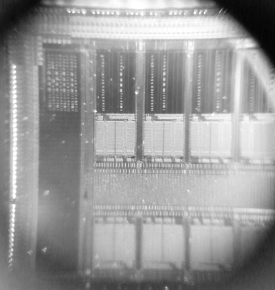
Even to the naked eye it's easy to spot which die was in which chip, like with the original ones:
On the right is "LSPC", which only contains logic gates and routing lines. Apart from the power supply rings and I/O buffers, the main area just looks like a carpet with no distinguishable structure. A close look reveals the multitude of logic cells (clear rectangles) and the noisy looking "interconnect" around them. It would be impossible to know if the logic exactly matches the original LSPC2-A2 one without comparing each and every cell.
The fact that the chip is from a different manufacturer, forcibly using a different cell library, even maybe at a different technology node, actually makes any comparison difficult. We only have the confirmation that the chip isn't a mask clone, and that it's a gate array. This means that the bootleggers either had to reverse-engineer the original chip to provide the manufacturer with an "anonymous" design, or they somehow got hold of an RTL description or internal schematic from SNK which they cleaned up or disguised as their own.

Without a real microscope I was only able to spot this marking in a corner, which might be the only one on the entire die as inserting "graphics" right in the middle of logic doesn't seem like common practice/possible in gate arrays:

Varying the light intensity, color and angle, this is the best shot I could get of it. TW1393-1086 ? Whatever that means. Maybe it's "TH" or "TM" and I'm biased towards thinking "TW" means Taiwan. See below for another shot making me lean towards "TW". Anyways, still no logo or clearer indication of who might be the manufacturer.
On the left is "CHIP23", visibly different because of the multiple line buffers RAM cells taking a lot of the surface. These are often called "macrocells": ready-made blocks available in multiple sizes which can be connected to the rest of the circuit just like logic cells. These RAM blocks can also be easily spotted in NEO-B1, although in a different arrangement because of the different manufacturer.
The die wouldn't fit entirely under the lens because of its slightly larger area but the four quadrants basically have the same appearance.
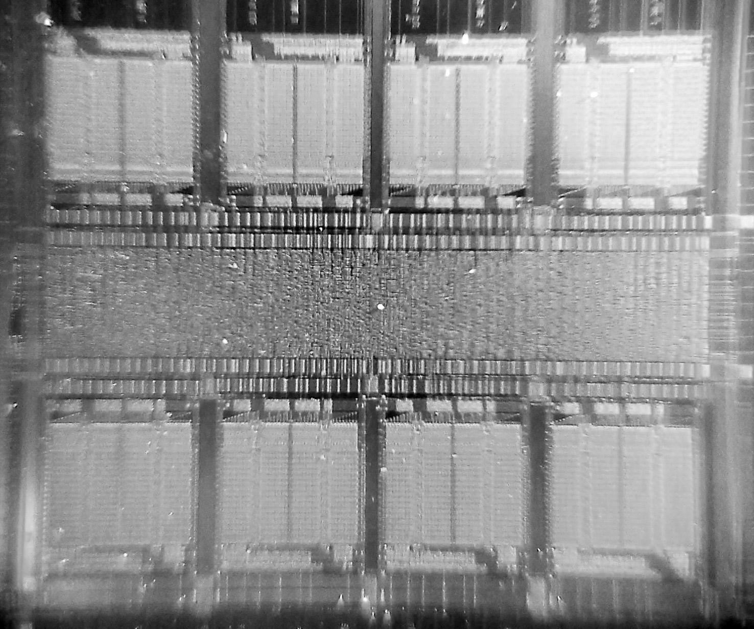
The center zone seems to hold everything: 8 RAM cells and a stuffed logic carpet zone:
The original NEO-B1 contains relatively simple and repetitive logic only used to latch wide buses and do some light multiplexing. Even if it was obvious by looking at the PCB that "CHIP23" integrated more logic than NEO-B1, it's still hard to know how much more it is just by taking an overall look.
The logic cells zone is visibly denser than in LSPC, but also less spread out.
Not seeing any interconnect makes me think this zone just contains unused master slice structures. They're present in all 4 corners.

Marking:
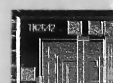
TW2642 ?


