Dumping the NEC PC Engine YUV table
This page is about a small part of a long story which involved several people.
Its chronology is laid out in detail in this RetroRGB post by Dan Mons.

In short, it had been observed that there were notable discrepancies between the RGB and YUV (composite) video outputs of the PC Engine / TurboGrafx-16.
My work was to check for the presence of a suspected color conversion table, and if it was, to extract its data.
Here's a very short summary of the PC Engine's video architecture:
The CPU tells the VDC (Video Display Controller) how the picture must be built: where the sprites must be, what tiles to use, how the layers are scrolled, etc...
As the VDC produces the image, it sends a stream of pixel color indices to the VCE, which uses them as an address to look up the needed color in the palette.
The VCE (Video Color Encoder) is responsible for generating the final analog RGB and YUV video signals.
It contains a palette RAM able to store 512 9-bit RGB color definitions: 3 bits for red, 3 for green, and 3 for blue, no surprises.

The palette RAM in the VCE can be accessed by both the VDC (for rendering) and by the CPU (for setting up the colors).
Priority is handled inside the VCE by a simple switch which ignores the VDC accesses when the CPU wants to read or write to the palette RAM, giving the CPU top priority.
The HuC6260 of a certified dead and unfixable PC Engine console was decapped and microscope observation revealed the expected blocks: some standard cell logic, SRAM, DACs and less expected ROM block (!).
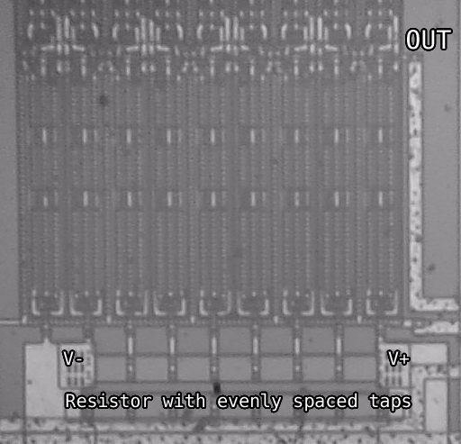
For the RGB output, the digital RGB data coming out of the palette RAM is directly converted to analog by three identical 3-bit DACs, one for each component.
These are string DACs (also called Kelvin dividers), where a long resistor is tapped by analog switches, one for each possible output value.
The 3-bit value is decoded to 2^3 = 8 "one-hot" lines, each selecting an output voltage.
Here for some reason the lowest intensity value (V- on the left) uses two switches in parallel, maybe for greater current handling.
In total there are 9 switches per DAC, which are the tall structures above the resistor:
For the YUV output however, since there's no easy way to convert from RGB without using time and space consuming hardware multipliers, it was strongly suspected that a lookup table was used.
Conversion from 3-bit linear RGB components to YUV gives values that would sit in between the possible analog steps of a 3-bit DAC. Such a low resolution conversion would cause colors to be poorly mapped across the YUV gamut. In practice however, this problem was observable but not as bad. This meant that the YUV outputs were either using higher precision DACs, or non-linear ones.
Following the YUV outputs pin pads provided the answer: they were all connected to linear 5-bit DACs, which have 2^5 = 32 steps, instead of 8 for RGB.
Here's one of the 3 YUV DACs, notice how bigger it is compared to those used for RGB:

At that point, I expected the 3 * 5 = 15 input data lines to simply come from the ROM block I had noticed earlier. Following one of those lines lead straight up to it, confirming that it held the data we were looking for.
The CPU can freely access the VCE's RGB palette memory for obvious reasons. However, being able to read or modify the YUV lookup table from the CPU would make no sense, so it was implemented as a simple ROM stuck between the palette RAM outputs and the DACs.
In such old systems, data tables are often stored as mask ROM, where the data bits are stored as transistors connected one way or the other.
The patterns formed by the orientation of the transistors makes optical reading or the data tedious, but possible.
Unfortunately, even by changing the light source and using the highest magnification, the ROM block present in the VCE showed no clear variations.
Obfuscation by hiding the data under one of the metal layers was very unlikely as there was no reason to, and both metal layers were obviously for used for routing anyway.
Then I remembered reading about the troubles of optically dumping implant ROM. This is a more advanced process used to make ROMs more compact, by storing the data as nearly invisible silicon doping differences instead of changing the shape of the layers.
The effort would have ended up failing here if there wasn't another way to read the ROM.
Looking back in slight despair at the data bus between the ROM and the DACs, I noticed junction points that I had first missed. The whole bus actually forked to some logic cells, meaning that some other part of the VCE was able to use the ROM's output. If that didn't lead to chopped-off test lines (some were seen in the HuC6270), this was looking a lot like a test mode that was left functional.
The ROM data lines fork to groups of 2-to-1 multiplexers forming two switching stages back to back, effectively forming 3-to-1 muxes.
The first selects the upper or the lower half of the 15 YUV ROM data bits (the 16th bit is fixed to zero), so that they fit nicely on a 8-bit bus, the same size as the CPU data bus. That's interesting.
The second set of muxes select between the palette RAM data or the previously split YUV table data. Even more interesting, this means something is physically able to access both the palette data and the YUV table data.
Following the final output bus led to the CPU data pin outputs drivers, confirming that there was indeed a path between the ROM output and the CPU.

Now I needed to know how these muxes were controlled. The two purple traces labelled "Select A" and "Select B" control the two mux stages.
Following them led to a small group of logic cells, quickly identified as buffers and AND gates thanks to their small size and IO count.

The red traces are connected to a "fixed level" cell, effectively providing a constant "logic high" level.
The other inputs simply come from the pin 58 and pin 59 pads, which are coincidentally unlabelled on the PC Engine schematics found on Console5.
Since the AND cells have one of their inputs always set high, this circuit simply buffers the inputs from pin 58 and 59 to the Select A and Select B signals.
Pin 60 is used for another test function that didn't end up useful for our purpose.
The apparently useless AND cells might have been used to provide an easy way of disabling the test pins in silicon if that needed to be done for some reason: they would have just had to set the common "high" signal to "low".
In the same way, I expected the ROM readout test mode to also route the CPU's address bus to the ROM instead of the palette RAM, to allow reading it in software.
For some unknown reason, it took me a while to understand that it was even simpler than that.
At this point I had a really bad brain fart and turned on the soldering iron instead of spending a few minutes more on the die pictures.
I undertook the task of desoldering the HuC6260 to spaghetti-wire it to a memory programmer with its test pins correctly set, in order to read it like regular ROM chip.

This didn't give any sensible values and even worse, data changed from read to read if the power was cycled. It's only a few days later that I realized what I did wrong, and that I could just have left the chip on the board to be read via the console's own CPU.
Test pins are typically used once during manufacturing and then never again. For example they may enable test modes exposing internal signals by re-purposing pins, to test long counters faster, to get characteristics of analog circuits, or... to check the integrity of internal memories.
Once the chip is tested and confirmed functional, it's soldered on the board with the test pins tied to a power rail to make sure the test functions are kept disabled forever.
Because it's intended to be used only once, it's desirable for the test mode logic to take the smallest area possible to reduce costs. Since the chip is going to be tested in a special test rig before being soldered, there's no particular need for the YUV ROM to be addressable from the CPU address bus.
So to avoid adding useless switches for the address bus on the silicon, they simply left the ROM connected to the palette RAM output.
This means that instead of seeing the YUV ROM mapped in place of the palette RAM and reading it like so by the CPU as I was expecting, it is actually addressed BY the palette RAM's output, effectively doing a double lookup. It makes the reading process slightly more complicated but it allowed Hudson to save silicon area.

So with the stupid spaghettis removed and the chip soldered back on the board with the right test mode enabled, the CPU can read the YUV ROM instead of the palette RAM.
Because of the double-lookup through the palette RAM, there has to be some control over which color index is being output from the VDC when the CPU performs the read in order to read from the ROM address we want.
Here are the paths when the HuC6260 is in its normal, non-test mode:

The VDC or the CPU can set the palette RAM address, and the CPU can read from/write to it.
The palette RAM outputs (the 9-bit RGB values) go to both the RGB DACs, and to the YUV ROM address inputs.
The YUV ROM then outputs its data to the YUV DACs.
When the ROM dump test mode is enabled, a path appears between the YUV ROM data bus and the CPU bus.
Since the ROM data is 15-bit, a second test pin is used to select between the upper or lower bits. There's no software control over this.

The simplest way I found to dump the ROM in software, is to clear the entire display so that only a single color is shown, and read the YUV ROM whenever the display is active (not in blanking periods, because the special black output could interfere).
- Enable YUV ROM readout mode by wiring test pins as necessary.
- Clear entire display, no sprites, no scrolling layers.
- Wait for v-blank interrupt.
- Set backdrop color value to the ROM address we want to read.
- Read from the "palette RAM" which is actually the ROM data now, store value in work RAM.
- Increment address.
- Repeat steps 3 to 7, 512 times (epilepsy warning).
- Setup a simple UI to visualize the 512 previously read values.
Thanks to the nice online documentation about PC-Engine programming, I was able to write a small program to perform these steps and then just slapped it on my Everdrive.
Since there's no way to control the lower/upper bits selection in software, I repeated the readback procedure with pin 59 wired to VCC instead of GND.
This gave a totally different set of values, which confirmed that the internal mux was working.
Here are the 512, 8 lower bits of the ROM. The topmost row is an hex index ($0 to $1F8, 24 values per column).

And the same for the 7 upper bits:

Putting the low and high bits together in a 512 * 15-bit table gave sensible YUV approximations of the RGB values.
I could have been clever and used raster interrupts or other trickery to read out the values quicker, but since I was unfamiliar with the system I didn't feel confident enough to go full smartass. Waiting 9 seconds instead of 1 wasn't that big of a deal anyway.
If you want to give it a go yourself, here's the readout ROM and its commented source code.


