This page is at least 6 years old !
Fujitsu CG10 Gate Array reverse-engineering
These pages are being written in parallel of my NeoGeo preservation project as an organized and publicly available (even if incomplete) reference for reverse-engineering Fujitsu CG10 series gate array chips by visually identifying cells and tracing connections from the bare die.
The layout of the CG10 cells may be identical to those of other series of the same period, like UHB and CG24.
 Legal info: Fujitsu owns patents regarding the master slice structure of their gate arrays. The cell layouts don't seem to be subject to patents but they might be copyrighted as regular mask work. If formally requested, I will take down proprietary information. The present data isn't guaranteed to be fully exact as most of it doesn't come from Fujitsu but from error prone reverse-engineering work. Use at your own risk.
Cell pictures were cropped from the NeoGeo's main graphics chip LSPC2-A2 die, which was imaged by John McMaster (siliconpr0n.org).
Pretty useful files
The CG10 part of the Fujitsu Databook (PDF)
A sorted list of all the available cells with their size and I/O count (ODS)
CG10 are 0.8µm CMOS channelled gate arrays with dual columns. This means the whole structure is made of alternating transistor-filled and empty columns for routing. Each transistor column is made of many rows of two Basic Cells ("BC", a group of 4 transistors) set side by side.
For example, LSPC2-A2 uses the CG10103 master slice, which is one of the largest in the series. It has 21 columns and 291 rows of BC pairs, so 12222 BCs in total. Fujitsu gives a maximum of 11080 usable gates as an estimation for a real, functional design.
The databook explains the architecture clearly:

The raw master slice doesn't do anything as the BCs aren't interconnected at all. Customization is done by placing pre-designed Unit Cells and connecting them together. Note that a unit cell is made of one or multiple Basic Cells.
Placement of unit cells is done by connecting BCs with a pre-designed metal layout, forming a tightly routed block somewhere in a column. Similarly to a regular integrated circuit, the unit cell has inputs and outputs "pins" to which more metal traces will be routed to connect to other unit cells.
Luckily, there aren't that many different unit cells. This means that most of the time, it's not necessary to go down to the transistor level to figure out what they do. Also, once a unit cell is identified, it can quickly be matched with others visually by looking for similar metal patterns and I/O connections. It seems like unit cells can be turned 180° but are never seen mirrored.
The CG10 Basic Cell
Here's an empty CG10 Basic Cell:

- A/B: Power supplies on Metal 2. Either VCC/GND or GND/VCC.
In CG10 chips, with two BCs side by, the power supplies are always VCC-GND-GND-VCC from left to right. - C and D: Transistor gates on Polysilicon. There are two transistors using the same gate.
- E and F: Diffusion. There's a gap between each BC, they're all isolated.
Loading Units
The databook mentions Loading Units ("lu"). These values indicate how many are used per input, and how many are available per output.
Think about TTL fanout. One output will only have enough "strength" to drive so many inputs.
For example, a 18lu output will be able to drive eighteen 1lu inputs. Or nine 2lu inputs... You get the idea.
Most of the CG10 unit cells inputs are 1 or 2lu, and the outputs seem to go from 6 up to 36. It all depends on how Fujitsu engineers designed them. Some unit cells provide the exact same logic function but are declined in multiple drive capabilities, to allow tradeoffs between BC usage (area) and output strength.
How many lu an input uses can be known by finding how many gates it drives. A pair of transistors will require 1lu.
If the input doesn't go to gates only, it can get a bit more complex.
How many lu an output allows can be known in a similar manner, by finding how many transistors drive it in parallel.
Gathering clues for identification
- Size of the cell (BCs used). Counting is easy when unit cells are clearly separated with unused BCs. When unit cells are packed together in dense gate arrays, some attention is needed to figure out how the cells are delimited.
- Number of inputs and outputs. Some common patterns give clues about the direction of a connection.
- Loading of inputs, driving capability of outputs. Thank the databook ! See below.
- Clock lines distributed vertically in bus-wide unit cells.
- When in doubt and if the databook gives the schematics of the plausible cells, try to map a few transistors starting from inputs or outputs to differentiate them.
Identifying a simple cell
Here's a simple unit cell using only 1 BC. See how metal (white traces) was added on top of the empty BC:

With a bit of imagination and the help of diagrams from the databook and patents, a layer decomposition can be drawn:

Black dots are vias ("nails" going through layers, like on PCBs).
Light grey is Metal 1 (M1), dark grey is Metal 2 (M2).
Orange is Polysilicon, the gate of the transistors.
Green is Diffusion.
First of all, just by knowing that the cell is only 1 BC in size, we know it won't be doing something complicated like arithmetic and that the function will only need 4 transistors at most.
The Fujitsu databooks lists only 5 cells which are 1 BC in size, so elimination can be a quick process.

By looking at the layers, we can see that there are only two "outside" connections: one horizontal trace on M1 going out the right side, and another one on M2 right below, at the bottom right.
Note the "ear" on M2 at the bottom left. That shape is part of the cell's layout and means a connection could have been done there.
For some reason, there are no such shapes at the top, even if they would connect to the same net.
Now we know that there are only 2 connections. This gets rid of the cells having 3 (N2N and R2N), leaving 3 possibilities:
- B1N, a true buffer (non-inverting).
- V1N, an inverter.
- V2B, a power inverter.
Let's look at the data pages for those:
- For B1N, the input loading is 1lu, the output drive is 18lu.
- For V1N, it's the same.
- For V2B, the input loading is 2lu, the output drive is 36lu.
By looking at the layers, we can see that the input is connected to both polysilicon zones, meaning it drives 2 pairs of transistors. It's a 2lu input.
We can also see that the output is connected to both diffusion zones, meaning it's driven by 2 pairs of transistors. It's a 9*2*2 = 36lu output.
Only one unit cell matches these characteristics: V2B ! It's a simple inverter.
"Power" just means that there's also another similar cell with less drive capability (in this case it's V1N, which only gives 18lu).
Without going down to trace the schematic at the transistor level, it was possible to identify the unit cell and its I/O locations.
Blind vias
Here's another V2B unit cell. This time it's turned around so that the input "ears" are at the top.

The input contact is at the top left. The output is still the center horizontal line, going out the left side this time.
See how the input metal trace runs over the vertical power supply traces.
The power supply vias circled in black are still visible through it, but they only connect M2 to the diffusion areas below.
They aren't connected to the input trace (otherwise it would connect it to VCC and GND !).
Understanding a larger cell
For a few cells, characteristics given by the databook are all identical. Therefore it is necessary to look at what the transistors are really doing to differentiate them.
For example, here's a unit cell 3 BC in size:

The databook lists 16 (!) cells having the same size.
There are 3 traces going directly to polysilicon, one coming from the right and two from the left. Those are 3 inputs.
There's one trace leaving to the left, coming from the middle of BCs. That's probably an output.
Knowing that, the list is cut down to only 6 cells.
Each of the 3 inputs only connect to a single polysilicon zone, so they're 1lu inputs.
The output drive is quite difficult to see, as the output trace goes over a lot of stuff.
In the list, only 4 cells have 1lu inputs:
- N3B: Power 3-input NAND
- N3P: Power 3-input AND
- R3B: Power 3-input NOR
- R3P: Power 3-input OR
Having no other criteria to shorten the list, let's trace the schematic. Here are the layers and annotations for inputs, outputs, power supplies and transistor numbers I used:

Admittedly, this can require some eye squinting and multiple tries. If power supplies end up being shorted, you know that something's wrong.
Apart from the M1/M2 confusion, another source of mistakes can be blind vias.
For example, the pair of vias just below the "Q1" text connects M2 with the diffusion zone only, it does not connect to M1 (the IN1 trace) !
I didn't find a viable way of knowing which layers a via goes through except by guessing from the overall structure. Again, this process can take a few tries before obtaining a schematic that makes sense.
Simply put, transistors are formed when polysilicon goes over diffusion. Those green zones are actually cut beneath the orange ones. When the transistor is turned off, no current flows because of the cut. When the transistor is on, current flows "over" the cut thanks to the voltage applied to the polysilicon (and physics principles I don't really understand...).
Here's the schematic of this mysterious unit cell:

As observed earlier, each of the 3 inputs go to a pair of transistors.
Q1, Q3 and Q7 are wired in parallel to VCC. Q2, Q4 and Q8 are wired in series to GND.
Both of those groups are wired together to a common net, which finally drives Q5, Q6, Q9 and Q10.
For that net to be connected to VCC (binary 1), any of the Q1, Q3 or Q5 transistors must be on. So any of the inputs must be binary 0.
For the same net to be connected to GND (binary 0), each of Q2, Q4 and Q8 must be on at the same time. So all the inputs must be binary 1.
If this unit cell was only made of those 6 transistors, it would be a 3-input NAND gate !
But it doesn't stop there, the net continues to two identical pairs of transistors (Q5/Q6 and Q9/Q10) forming two inverters wired in parallel, which gives the cell's final output. Invert the output of a NAND gate and you get an AND gate.
This cell is N3P: Power 3-input AND ! How cute is that ?

Note how they call it a "power" gate also, as the output uses 2 pairs of transistors for a higher driving capability.
This sort of parallel/series topology can help identify simple gates:
- NAND has VCC in parallel, GND in series.
- NOR has GND in parallel, VCC in series.
- AND and OR are the same with an added inverter on the output.
Luckily, the bigger cells have unique data so identifying them doesn't require doing that for hundreds of transistors.
To trace out LSPC2, the biggest cell which required that kind of work was only 8 BC in size.
Visual cell library
Work in progress, come back for more pictures ! Red are inputs, Green are outputs.
| Name | Description | Size | Inputs | Outputs | Mugshot |
|---|---|---|---|---|---|
| A4H | 4-bit Binary Full Adder with Fast Carry | 48 | 9 | 5 | |
| B1N | True Buffer | 1 | 1 | 1 | |
| BD3 | True Delay Buffer (>5ns) | 5 | 1 | 1 | 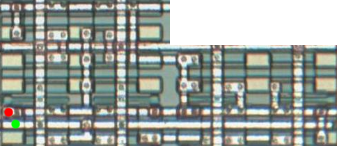 |
| BD5 | True Delay Buffer (>10ns) | 9 | 1 | 1 |  |
| C43 | Non-SCAN 4-bit Binary Synchronous Up Counter | 48 | 9 | 5 |  |
| D24 | 2-wide 2-AND 4-input AOI | 2 | 4 | 2 |  |
| FD2 | Non-SCAN Power DFF | 7 | 2 | 2 |  |
| FDM | Non-SCAN DFF | 6 | 2 | 2 |  |
| FDP | Non-SCAN DFF with Set and Reset | 8 | 4 | 2 | 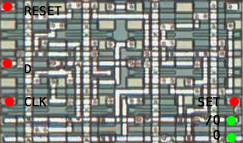 |
| FDR | Non-SCAN 4-bit DFF with CLEAR | 26 | 6 | 5 | |
| FDS | Non-SCAN 4-bit DF | 20 | 5 | 4 |  |
| FS1 | 4-bit Serial-in Parallel-out Shift Register | 18 | 2 | 4 | |
| FS2 | 4-bit Shift Register with Synchronous Load | 30 | 7 | 4 | |
| I2B | Input buffer | 4 | 1 | 1 |  |
| N2B | Power 2-input NAND | 3 | 2 | 1 | |
| N2K | Fast Power 2-input NAND | 2 | 2 | 1 |  |
| N2P | Power 2-input AND | 2 | 2 | 1 |  |
| N3K | Power 3-input NAND | 3 | 3 | 1 |  |
| N3P | Power 3-input AND | 3 | 3 | 1 | 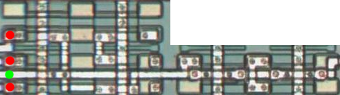 |
| N4K | Power 4-input NAND | 4 | 4 | 1 |  |
| N4P | Power 4-input AND | 3 | 4 | 1 |  |
| O2B | Output Buffer | 2 | 1 | 2 |  |
| O4TF | 3-state Output Buffer | 4 | 2 | 2 |  |
| R2K | Power 2-input NOR | 2 | 2 | 1 |  |
| R2P | Power 2-input OR | 2 | 2 | 1 |  |
| R3K | Power 3-input NOR | 3 | 3 | 1 | 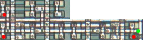 |
| T2B | 2:1 Selector | 2 | 4 | 1 |  |
| T2E | Dual 2:1 Selector | 5 | 5 | 2 |  |
| T5A | 4:1 Selector | 5 | 10 | 1 |  |
| T44 | Power 4-AND 4-wide Multiplexer | 11 | 16 | 1 | |
| V2B | Power Inverter | 1 | 1 | 1 |  |
| X1B | Power Exclusive NOR | 4 | 2 | 1 |  |
| X2B | Power Exclusive OR | 4 | 2 | 1 |  |


